

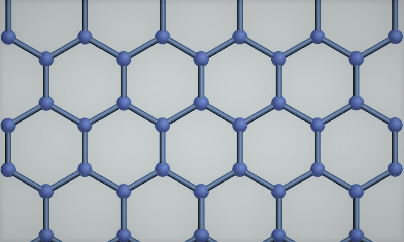
Graphite, or pencil lead, is a layered material made up of loosely held together sheets of single atom thick carbon, called graphene.
However, it was not until 2004 that scientists proved they could isolate a single graphene sheet from the graphite bulk and produce a nearly transparent and hyperflexible conductive material with exotic physical properties.
In fact, many naturally occurring layered materials, known as van der Waals materials, can be thinned down to their atomically thin component layers in the exact same way. And – while graphene is conductive – semiconductors are required in order to make common electronics, such as switches (transistors) and LEDs.
Luckily, graphene has several semiconducting cousins that can be peeled apart in the same way, including materials whose individual layers are a sandwich of selenium or sulfur, with a metal in the middle. Two of these are materials that I work with: molybdenum disulfide and tungsten disulfide.
The ways these materials are typically produced for lab experiments involves peeling the layers apart with sticky tape – a method that has been used for more than a decade. Peeling the material produces little flakes of random sizes (usually not larger than 5 micrometres on a side) and random shapes in random locations.
Plenty of effort also goes into methods for growing these materials instead, but until very recently the electronic quality of the grown material was not as good as the peeled material.