Recently, beta gallium oxide (β-Ga2O3) has received much attention due to its potential to dramatically improve wide bandgap semiconductor device applications in power electronics, UV solar blind detectors, and gas sensors. Wide bandgap energy (∼4.9 eV), and high breakdown voltage (8 MV/cm) make β-Ga2O3 an outstanding candidate material for next generation power electronics. The thermal stability of β-Ga2O3 facilitates the development of gas sensors operable at high temperatures. Realizing the potential of β-Ga2O3 for electronic and optical devices relies on the ability to control material properties and the development of material synthesis and processing techniques. Ultrafast (femtosecond pulse) laser processing provides a unique means of material modification which may provide a new pathway for β-Ga2O3 material synthesis and processing. The feasibility of irradiation in air ambient and direct laser writing provide opportunities for flexibility in material processing and low-cost processing approaches. Moreover, the femtosecond time scale allows transparent materials to absorb irradiation at sub-bandgap energy through nonlinear processes, leading to a nonequilibrium state between free electrons and phonons. This nonequilibrium state can eventually be stabilized by the formation of surface nanostructures such as laser-induced periodic surface structures (LIPSS) at a high spatial frequency (HSFL). Furthermore, enhanced atomic drift associated with the high density of excited electrons can result in the generation of permanent point defects.
The unique material interactions associated with ultrafast laser irradiation contribute to many applications. Modified surface and optical properties resulting from nanostructuring may be used to realize colorization and surface texturing.The intentional introduction of point defects via ultrafast laser irradiation may also provide an opportunity to overcome challenges in the controlled doping of wide bandgap materials such as β-Ga2O3 by incorporating impurities into these point defects under nonequilibrium conditions introduced via femtosecond laser irradiation. Ultrafast laser irradiation on 4H-SiC, one of the widely utilized wide bandgap semiconductor materials, demonstrated electrical modification in the form of increased lateral conductance over orders of magnitude.
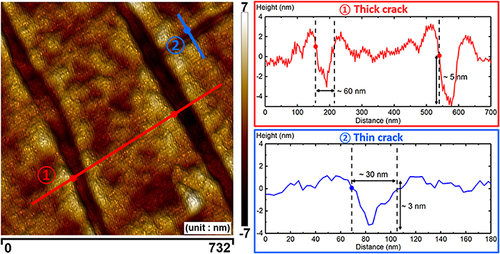
Nakanishi et al. reported that the formation of nanogrooves under multiple femtosecond double-pulse irradiation focused on the laser beam at the depth of 100 μm from sample surface where the pulse energy (7.5 μJ per single pulse) is lower than the surface damage threshold (22 μJ for single pulse from this work). In contrast, our work focuses on a higher fluence regime near the damage threshold, and directly on surface modifications, where morphology differs dramatically from Nakanishi et al. Several damage thresholds of β-Ga2O3 associated with the generation of highly aligned straight thermal cracks and ablation are reported which can be interpreted as single exposure femtosecond laser-induced damage threshold (LIDT). The cracking behavior is observed for single pulse irradiation and without observable structural phase change of the initial β-Ga2O3 material. In addition, HSFL are observed without phase transition under multiple pulse irradiation below the ablation threshold.


 TWITTER FEED