

Surface acoustic wave (SAW) resonators are low cost devices that can operate wirelessly on a received radio frequency (RF) signal with no requirement for an additional power source. Multiple SAW resonators operating as transponders that form a wireless sensor network (WSN), often need to operate at tightly spaced, different frequencies inside the industrial, scientific and medical (ISM) bands. This requires nanometer precision in the design and fabrication processes. Here, we present results demonstrating a reliable and repeatable fabrication process that yields at least four arrays on a single 4-inch wafer. Each array consists of four single-port resonators with center frequencies allocated inside four different sub-bands that have less than 50 kHz bandwidth and quality factors exceeding 8000. We see promise of standard, low-cost photolithography techniques being used to fabricate multiple SAW resonators with different center resonances all inside the 433.05 MHz–434.79 MHz ISM band and a mere 100 kHz spacing. We achieved that by leveraging the intrinsic process variation of photolithography and the impact of the metallization ratio and metal thickness in rendering distinct resonant frequencies.
A triboelectric nanogenerator (TENG) is a new energy harvester that converts small scale mechanical motions into electrical energy by a combination of triboelectrification and electrostatic induction through the periodic contact-separation and/or sliding movement between two tribo-materials with different abilities of gaining or losing electrical charges.
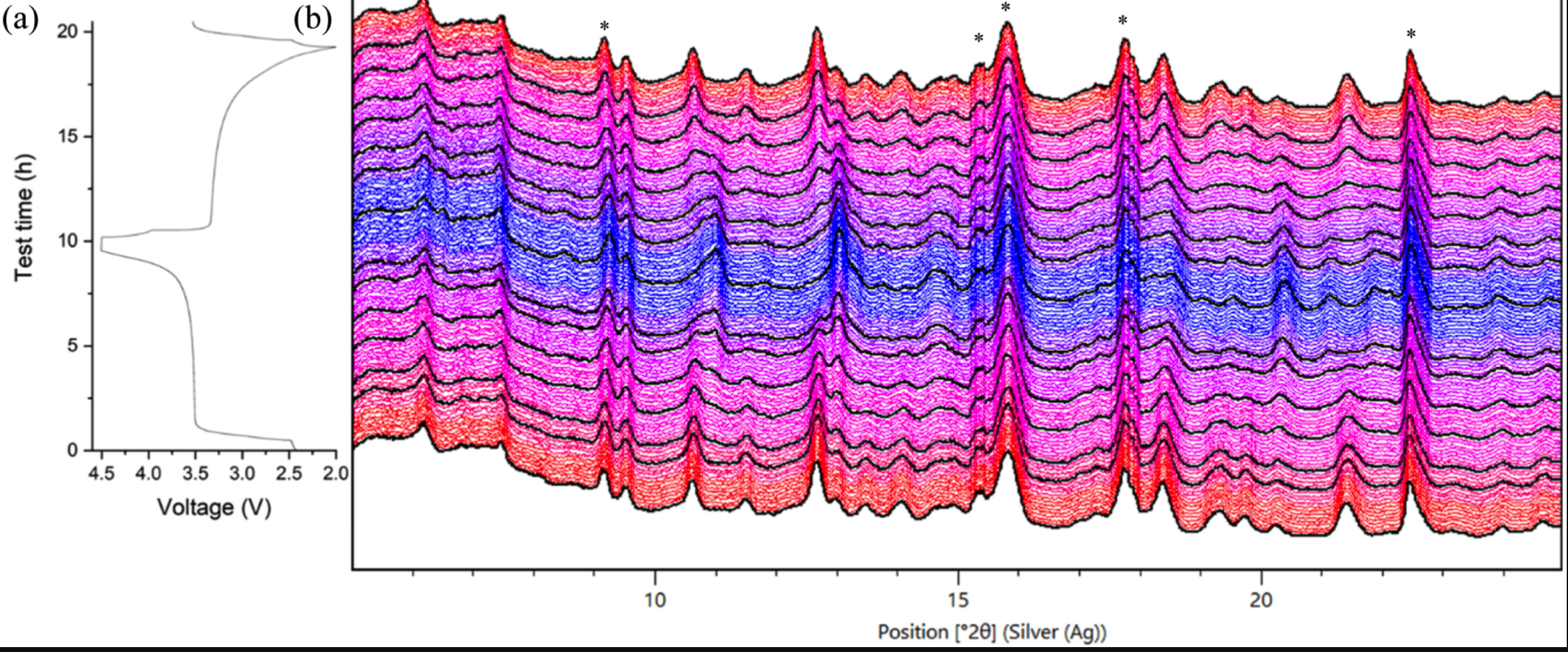
We have used a laboratory diffractometer to perform operando X-ray diffraction on LiFePO4 during electrochemical cycling in a coin cell fitted with a Kapton window. The results obtained are in good agreement with previous studies, verifying that extraction of Li from LiFePO4 follows dual-phase solid solution behaviour, with neither LiFePO4 nor FePO4 maintaining a static composition during deintercalation.
While the importance of atomic-scale features in silicon-based device for quantum application has been recognized and even the placement of a single atom is now feasible, the role of a dopant in the substrate has not attracted much attention in the context of quantum technology. In this paper, we report random telegraph signals (RTSs) originated from trapping and detrapping of an electron by a donor in the substrate of a p-type metal–oxide–semiconductor field-effect-transistor. RTSs, not seen when the substrate was grounded, were observed when a positive bias was applied to the substrate. The comprehensive study on the signals observed reveals that the nature of the RTSs is discrete threshold voltage variations due to the change in the depletion layer width depending on the charge state of a single dopant, neutral or positively charged.
In this work, the working performance of Platinum (Pt), solvent-free nanoparticle (NP)-based strain sensors made on a flexible substrate has been studied. First, a new model has been developed in order to explain sensor behaviour under strain in a more effective manner than what has been previously reported.

ICON has evolved into a truly unique international programme, spearheaded by our PhD students distributed across global institutions. We are immensely proud of all of our students that excel in their research and are recognised by awards, impactful publications and engagements with world-leading industry and societies – as highlighted here. Our commitment for enhancing their skills and experiences was reinforced through our Distinguished Lecture series, given this year by Dr Shaun Fitzgerald, Director of the Royal Institution, focussing on public engagement with science. Building on our previous successes with Nanotechnology outreach, we continued to develop our 'Introducing the Nanoworld' experience. And last but not least, we are particularly thankful to Professor Koh and colleagues, for so graciously hosting our summer school at the Lloyd's Register Foundation Institute for the Public Understanding of Risk.
Ultrafast (femtosecond pulse) laser irradiation provides unique laser-material interactions associated with high instantaneous electric fields and short timescales that lead to a nonequilibrium state between excited electrons and phonons. These interactions result in material modifications that differ from conventional chemical, physical, and thermal processing at much longer timescales, and an opportunity to address material and device processing challenges associated with wide-bandgap materials such as Ga2O3.

Halide perovskite materials have promising performance characteristics for low-cost optoelectronic applications. Photovoltaic devices fabricated from perovskite absorbers have reached power conversion efficiencies above 25 per cent in single-junction devices and 28 per cent in tandem devices. This strong performance (albeit below the practical limits of about 30 per cent and 35 per cent, respectively is surprising in thin films processed from solution at low-temperature, a method that generally produces abundant crystalline defects.
Nowadays, the Internet‐of‐Things (IoT)‐related applications require the design of low‐cost and low‐power wireless sensor nodes. Although backscatter radio communication is a mature technology used in radio frequency identification (RFID) applications, ambient backscattering is a novel approach taking advantage of ambient signals to simplify wireless system topologies to just a sensor node and a receiver circuit eliminating the need for a dedicated carrier source.
Environmental and safety sensing is becoming increasingly important in the oil and gas industry. However, present solutions to feed theses sensors are expensive and dangerous and there is so far no technology able to generate electrical energy in the operational conditions of oil and gas extraction wells. Here, we show that triboelectric nanogenerators (TENGs) can withstand and harvest energy in harsh conditions.
Titanium dioxide represents one of the most widely studied transition metal oxides due to its high chemical stability, non-toxicity, abundance, electron transport capability in many classes of optoelectronic devices and excellent photocatalytic properties. Nevertheless, the wide bang gap of pristine oxide reduces its electron transport ability and photocatalytic activity. Doping with halides and other elements has been proven an efficient defect engineering strategy in order to reduce the band gap and maximize the photocatalytic activity. In the present study, we apply Density Functional Theory to investigate the influence of fluorine and chlorine doping on the electronic properties of TiO2. Furthermore, we present a complete investigation of spin polarized density functional theory of the (001) surface doped with F and Cl in order to elaborate changes in the electronic structure and compare them with the bulk TiO2.
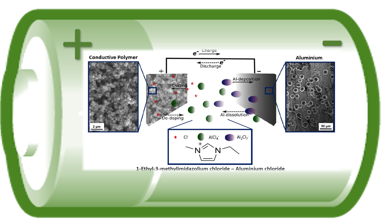
Aluminium batteries with non-aqueous electrolyte have initially focused on Lewis acidic ionic liquid systems with heavy Al2Cl7− anions that limit the specific capacity, energy and power. In order to develop the secondary aluminium batteries further for future energy storage beyond lithium-ion, high performance electrolytes that enable efficient aluminium deposition/dissolution must be developed. This work studied the electrodeposition of aluminium from both 1-ethyl-3-methylimidazolium chloride aluminium chloride (EMImCl-AlCl3) ionic liquids with different Lewis acidities, and their gel form- the ionogel.

A major challenge to routine non-invasive, nanoscale magnetic imaging is the development of Hall sensors that are stable under ambient conditions and retain low minimum detectable fields down to nanoscale dimensions. To address these issues we have fabricated and characterised chemical vapour deposition (CVD) graphene Hall sensors with wire widths between 50 nm and 1500 nm, in order to exploit the high carrier mobility and tuneability of this material. The measured Hall voltage noise is in good agreement with theoretical models and we demonstrate that minimum detectable fields at fixed drive current are lowest in the vicinity of the charge neutrality point. Our best performing deep sub-micron sensors, based on a wire width of 85 nm, display the excellent room temperature resolution of 59 µT/√Hz at a dc drive current of 12 µA and measurement frequency of 531 Hz. We observe a weak increase in minimum detectable field as the active sensor area is reduced while the Hall offset field is largely independent of size. These figures-of-merit significantly surpass prior results on larger probes in competing materials systems, with considerable scope for further optimisation. Our results clearly demonstrate the feasibility of using CVD graphene to realise very high spatial resolution nanosensors for quantitative room temperature magnetic imaging.
We show a manipulation of a single electron at room temperature by controlling Random Telegraph Signals (RTSs) by voltage pulses. Our silicon nanowire triple-gate transistor exhibited RTSs when potential barriers were electrically created by two of the three gates. From the statistics of the signals, we optimized the voltage pulse such that a single electron was intentionally captured in the potential well, and the retention time of approximately 10 ms was observed in this memory operation. This study indicates that a single electron effect can be controllable in a form of RTSs at room temperature by electrically defining a potential well.
Mixed‐halide lead perovskites have attracted significant attention in the field of photovoltaics and other optoelectronic applications due to their promising bandgap tunability and device performance. Here, the changes in photoluminescence and photoconductance of solution‐processed triple‐cation mixed‐halide (Cs0.06MA0.15FA0.79)Pb(Br0.4I0.6)3 perovskite films (MA: methylammonium, FA: formamidinium) are studied under solar‐equivalent illumination. It is found that the illumination leads to localized surface sites of iodide‐rich perovskite intermixed with passivating PbI2 material. Time‐ and spectrally resolved photoluminescence measurements reveal that photoexcited charges efficiently transfer to the passivated iodide‐rich perovskite surface layer, leading to high local carrier densities on these sites. The carriers on this surface layer therefore recombine with a high radiative efficiency, with the photoluminescence quantum efficiency of the film under solar excitation densities increasing from 3% to over 45%. At higher excitation densities, nonradiative Auger recombination starts to dominate due to the extremely high concentration of charges on the surface layer. This work reveals new insight into phase segregation of mixed‐halide mixed‐cation perovskites, as well as routes to highly luminescent films by controlling charge density and transfer in novel device structures.
Thermochromic vanadium dioxide (VO2) window coatings hold the promise of reducing the energy consumption of the built environment by passively regulating solar heat gain in response to changing conditions. Composite materials with embedded VO2 particles have shown greatly improved optical performances compared with thin films, however they typically exhibit broadened phase transition hysteresis and gradient widths, which negatively impacts the overall performance. Here, we present a scalable one-step solution based synthesis for a thermochromic smart window coating based on a vanadium dioxide sol-gel containing silica (SiO2 nanoparticles. We compare the performance of our nanoparticle composite with thin film VO2 along with composites formed by mixing VO2 and SiO2 sol-gels and find that both composites achieve an acceptable visible transmittance (∼ 50%) along with a comparable and competitive solar modulation (12.5% and 16.8% respectively), roughly double that of the plain VO2 film (6.7%). However, our SiO2 nanoparticle containing composite also benefits from a narrow transition hysteresis and gradient width (9.4 ∘C and 2.9 ∘C respectively). We predict that this method may subsequently be combined with metal ion doping to control both the optical and phase transition characteristics to achieve composite films with high overall energy saving performances.

We are delighted to see that during this year, ICON has evolved into a truly unique international action, spearheaded by our PhD students distributed across global institutions. We are immensely proud for all of our students that excel in their research and are recognised by awards, impactful publications and engagements with world-leading industry and societies – as highlighted in this report. Our commitment for enhancing their skills and experiences was reinforced through the establishment of a Distinguished Lecture series that are broadcast online and bring to our students exemplar role models for Nanosciences and Engineering. Building on our previous successes with Nanotechnology outreach, we partnered with the Royal Academy of Engineering that empowered us to promote our approach in a more diverse and broad manner (e.g. engaging secondary students for introducing “nano-concepts” to primary students). And we are particularly thankful to Dr Hayaatun Sillem, RAEng CEO, for sharing our vision and delivering the inaugural ICON distinguished lecture and motivating our ICON members via raising the importance of diversity in research.
Single crystal (010) β-Ga2O3 was irradiated by a Ti:sapphire ultrafast laser (150 fs pulse width) with varying fluences and a number of pulses in air ambient. Femtosecond laser-induced damage threshold of β-Ga2O3 is reported. Single pulse exposure results in surface morphological changes above a threshold laser fluence of 1.11 J/cm2. Laser-induced straight cracks aligned to the [001] crystallographic direction are observed in the laser irradiated regions, which are believed to be caused by laser-induced thermal stress, due to the unique low thermal conductivity and anisotropy associated with β-Ga2O3. Multiple pulse irradiation below the single pulse damage threshold fluence exhibited the formation of high spatial frequency laser-induced periodic surface structures. Electron backscattering diffraction and Raman spectroscopy suggested that there was no apparent phase transition of the irradiated β-Ga2O3 material for either single pulse or multiple pulse irradiation. This work serves as a starting point to further understanding the material properties of β-Ga2O3 and to unlock the potential for ultrafast laser material processing of β-Ga2O3.
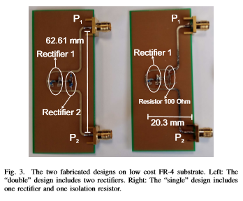
In this work a novel high efficiency, low-cost and low-complexity RF-to-dc converter was designed for RF energy harvesting in the 2.4 GHz band. The proposed design has two RF inputs and maintains a high efficiency over a wide range of incoming incident wave angles. The circuit is based on a Wilkinson power combiner and has two single-diode rectifiers. One rectifier is connected at the combiner’s output and collects the energy coming from the two inputs. The second rectifier replaces the isolation resistor of the combiner in order to collect the power that would otherwise be dissipated in it. The second rectifier is used for recycling the wasted power when the input signals do not have the same phase. The novel RF-to-dc converter was fabricated using commercially available components and low cost FR-4 substrate. A prototype was designed and its efficiency was optimized for low power input levels. The measured system efficiency was 16.2% for in-phase input signals with available input power −17 dBm. When the relative phase of input signals varied from 0 to 360 degrees, a variation in efficiency between 15.3% and 22% was observed. For input power 3 dBm, the efficiency varies from 26% to 39% between 0 to 360 degrees phase difference.
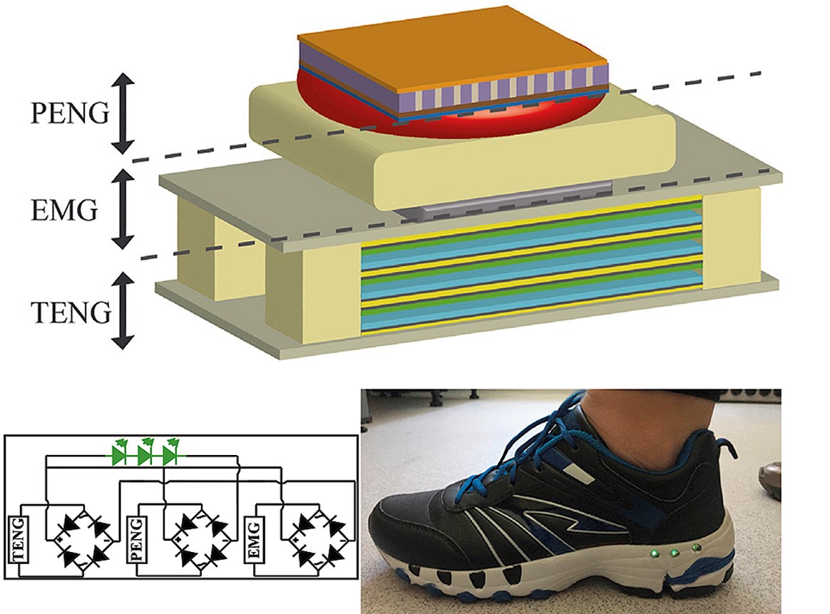
There is an increasing need to monitor in real-time health or wellbeing parameters such as heart rate, burned calories, walked steps, blood pressure, time spent exercising or athletic performance. To suit such demands, wearable and portable electronic devices are being developed and have attracted a large amount of attention in recent years. However, as the number of portable and wearable electronics increases, so does the need for new and independent power sources that allow a continuous operation of these small devices. In fact, present developments in electronics are making devices increasingly smaller and operating at ultra-low power consumption, opening the possibility to power them by energy harvested from our living environment.
This paper presents a new current attenuator circuit to scale down the inference currents in memristor based crossbars that drive integrate-and-fire neurons, which subsequently allows to reduce the size of integrating capacitors by several orders of magnitude, making IC integration possible. The proposed circuit uses a linear switch to divide the inference current and scale it down by a factor of about 10 4 . The proposed attenuator has been designed in 130nm CMOS technology. Simulation results considering noise, process and temperature variations are shown to validate the presented approach.
One source of instability in perovskite solar cells (PSCs) is interfacial defects, particularly those that exist between the perovskite and the hole transport layer (HTL). We demonstrate that thermally evaporated dopant-free tetracene (120 nm) on top of the perovskite layer, capped with a lithium-doped Spiro-OMeTAD layer (200 nm) and top gold electrode, offers an excellent hole-extracting stack with minimal interfacial defect levels. For a perovskite layer interfaced between these graded HTLs and a mesoporous TiO2 electron-extracting layer, its photoluminescence yield reaches 15% compared to 5% for the perovskite layer interfaced between TiO2 and Spiro-OMeTAD alone. For PSCs with graded HTL structure, we demonstrate efficiency of up to 21.6% and an extended power output of over 550 hours of continuous illumination at AM1.5G, retaining more than 90% of the initial performance and thus validating our approach. Our findings represent a breakthrough in the construction of stable PSCs with minimized nonradiative losses.
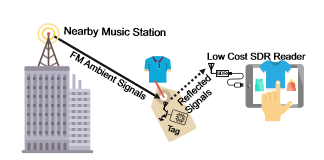
Nowadays, the monitoring of plant water stress is of high importance in smart agriculture. Instead of the traditional ground soil-moisture measurement, leaf sensing is a new technology, which is used for the detection of plants needing water. In this work, a novel, low-cost and low-power system for leaf sensing using a new plant backscatter sensor node/tag is presented. The latter, can result in the prevention of water waste (water-use efficiency), when is connected to an irrigation system. Specifically, the sensor measures the temperature differential between the leaf and the air, which is directly related to the plant water stress. Next, the tag collects the information from the leaf sensor through an analog-to-digital converter (ADC), and then, communicates remotely with a low-cost software-defined radio (SDR) reader using monostatic backscatter architecture. The tag consists of the sensor board, a microcontroller, an external timer and an RF front-end for communication. The timer produces a subcarrier frequency for simultaneous access of multiple tags. The proposed work could be scaled and be a part of a large backscatter wireless sensor network (WSN). The communication protocol exploits the low-complexity Morse code modulation on a 868 MHz carrier signal. The presented novel proof-of-consent prototype is batteryless and was powered by a flexible solar panel consuming power around 20 µW. The performance was validated in an indoors environment where wireless communication was successfully achieved up to 2 m distance.
Ambient backscatter uses radio frequency signals available in the environment (e.g. radio broadcasting, television or mobile telephony) to transmit data effectively leading to significant energy and cost efficiency increase. This paper presents a novel wireless tag, which for the first time utilizes 4-pulse amplitude modulation (4-PAM) technique to modulate the ambient backscattered FM signals in order to send data to a nearby low-cost software defined radio reader. The tag is based on an RF front-end that uses a single transistor controlled by an ultra low-power microcontroller. The microcontroller includes an analog-to-digital converter (ADC) for sensing and a digitalto-analog converter (DAC) for RF front-end control. A proofof-concept prototype is demonstrated in an indoor environment with the low bit rate of 345 bps and power consumption 27 µW. It operated using a real FM station at 34.5 Km away and the tagto-reader distance was tested at 1 m. The value of energy spent in this modulator was 78.2 nJ/bit at 345 bps and 27.7 nJ/bit at 10.2 Kbps.
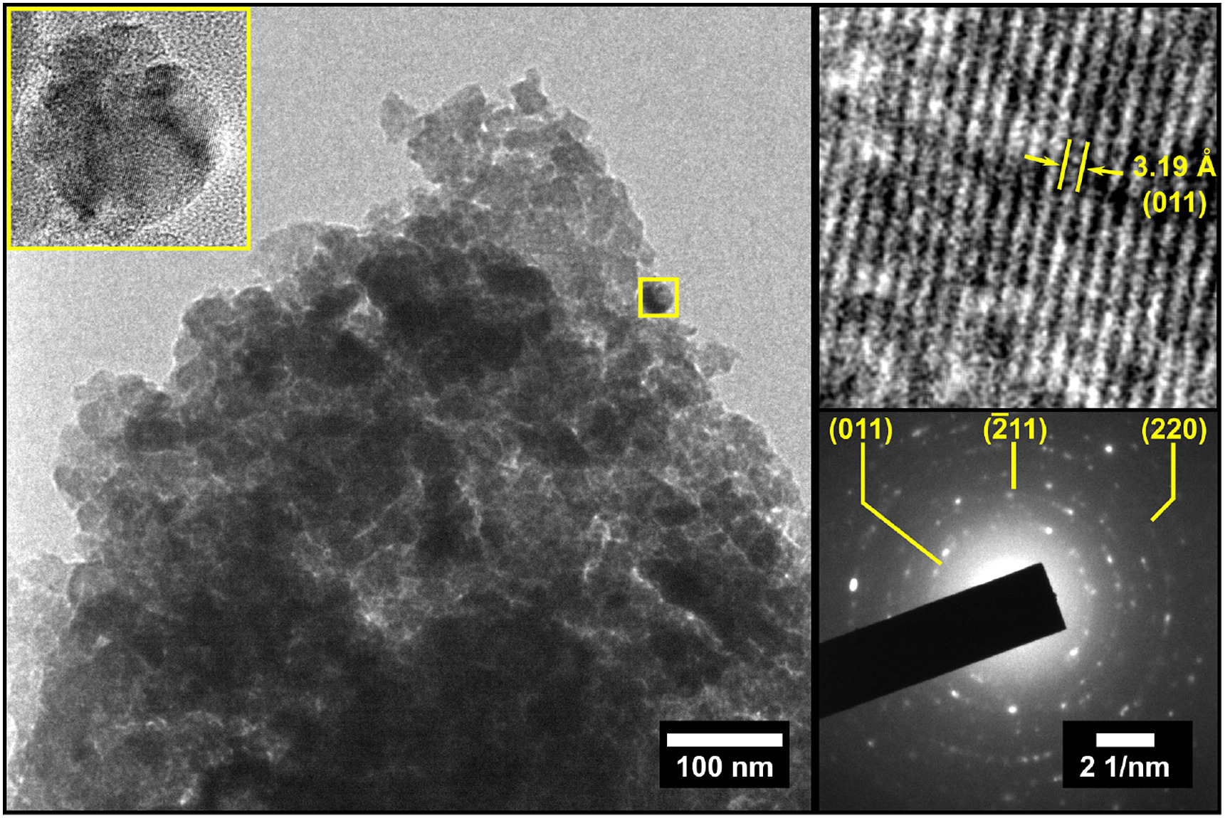
Carbon nanotube grafted carbon fibers (CNT-g-CFs) were prepared continuously, spool to spool, via thermal CVD. The application of an in-situ potential difference (300 V), between the fibers and a cylindrical graphite foil counter electrode, enhanced the growth, producing a uniform coverage of carbon nanotubes with diameter ca. 10 nm and length ca. 125 nm. Single fiber tensile tests show that this approach avoids the significant reduction of the underlying carbon fiber strengths, which is usually associated with CVD grafting processes. Single fiber fragmentation tests in epoxy, with in-situ video fragment detection, demonstrated that the CNT-g-CFs have the highest interfacial shear strength reported for such systems (101 ± 5 MPa), comparable to state-of-the-art sizing controls (103 ± 8 MPa). Single fiber pull-out data show similar trends. The short length of the grafted CNTs is particularly attractive for retaining the volume fraction of the primary fibers in composite applications. The results are compared with a short review of the interfacial data available for related systems.
We propose a new low VπL, fully-crystalline, accumulation modulator design based on a thin horizontal gate oxide slot fin waveguide, on bonded double Silicon-on-Insulator (SOI). A combination of anisotropic wet etching and the mirrored crystal alignment of the top and bottom SOI layers allows us for the first time to selectively pattern the bottom layer from above. Simulations presented herein show a VπL = 0.17Vcm. Fin-waveguides and passive Mach-Zehnder Interferometer (MZI) devices with fin-waveguide phase shifters have been fabricated, with the fin-waveguides having a transmission loss of 5.8dB/mm and a 13.5nm thick internal gate oxide slot.
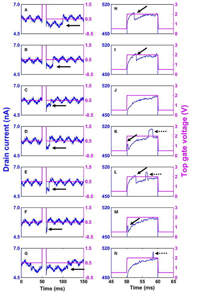
Manipulation of carrier densities at the single electron level is inevitable in modern silicon based transistors to ensure reliable circuit operation with sufficiently low threshold-voltage variations.
Safe and sustainable energy storage systems with the ability to perform efficiently during large numbers of charge/discharge cycles with minimum degradation define the main objective of near future energy storage technologies.
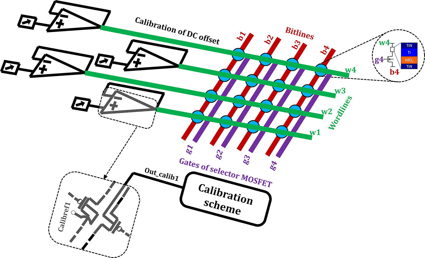
Neuromorphic RRAM circuits typically need currents of several mA when many binary memristive devices are activated at the same time. This is due to the low resistance state of these devices, which increases the power consumption and limits the scalability.

As you will read in these pages, our second year has been very exciting and impactful. We have significantly expanded our network of Lloyd’s Register Foundation Doctoral Students that are currently developing twenty-seven unique programs that surpass geographical and disciplinary boundaries. We are also attracting an exciting international audience, with strong industrial and policy making representation, willing to engage in the ICON network and growing this sustainably. We held our first annual conference in Athens Greece where all our students and stakeholders came together. We were delighted to see the drive in our students for describing their work and are thankful to our keynote speakers for engaging with our students and offering advice on future research and translation pathways

Metal halide perovskites are of great interest for various high-performance optoelectronic applications. The ability to tune the perovskite bandgap continuously by modifying the chemical composition opens up applications for perovskites as coloured emitters, in building-integrated photovoltaics, and as components of tandem photovoltaics to increase the power conversion efficiency.
The electrical properties of 4H-SiC under ultrafast laser irradiation in the low fluence regime (<0.50 J/cm2) are presented. The appearance of high spatial frequency laser induced periodic surface structures is observed at a fluence near 0.25 J/cm2 and above, with variability in environments like in air, nitrogen, and a vacuum.
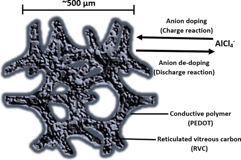
This work shows the electro-polymerisation of thin film poly(3,4-ethylenedioxythiophene) on three-dimensional reticulated vitreous carbon substrates by cyclic voltammetry and pulsed polymerisation methods from a Lewis neutral chloroaluminate ionic liquid containing 3,4-ethylenedioxythiophene monomer.
The FTO/TiO2 interface plays a crucial role in the performance of dye-sensitized solar cells (DSSCs). The uneven microstructure morphology of FTO (luorine-doped tin oxide) glass surface and high porosity of T iO2 layer produce tiny gaps and voids at the FTO/TiO2 interface that breaks the connectivity, leading to an increase in the recombination process. In the current work, a dual functional passivating layer is introduced by the combination of the graphene/TiO2 compact layer. The excellent mobility and lexibility of graphene is capitalized using its layer to ill the voids in the FTO surface, which can consequently reduce the charge transfer resistance at the interface, while the added T iO2 compact layer avoids direct contact with the electrolyte thus reducing the recombination. Graphene was synthesized by the facile solvent exfoliation method with the assistance of the probe sonication process. The parameters of sonication were optimized to achieve high-quality concentrated graphene inks (0.177–0.51 mg/ml). Raman spectroscopy and transmission electron microscopy (TEM) revealed that the graphene obtained is of a few-layer type. Electrochemical impedance spectroscopy (EIS) analysis indicated that the incorporated compact layer of graphene/TiO2 was capable of accelerating the charge transfer and reducing the recombination process at the FTO/TiO2 interface. Consequently, the photoconversion eiciency (PCE) for the device (1 cm2 active area) with double-coated graphene layer under one sun irradiation (AM 1.5) was found to be 33% higher than the conventional one.
This work studied the electro-polymerisation of 3,4-ethylenedioxythiophene (EDOT) and its electrochemical behavior in Lewis acidic, neutral and basic chloroaluminate ionic liquid 1-ethyl-3-methylimidazolium chloride aluminum chloride (EMImCl-AlCl3) by cyclic voltammetry. It was found that the electro-polymerisation on vitreous carbon only occurs in Lewis neutral EMImCl-AlCl3 as a dark blue-violet film whereas the electro-polymerisation in a Lewis acidic or basic compositions is not possible due to the interactions between the conductive polymer and the ionic liquid as well as the potential stability limits of the electrolyte.
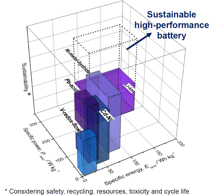
The main challenges to implement sustainable energy storage technologies are the utilization of earth-abundant recyclable materials, low costs, safe cell reactions and high performance, all in a single system. Aluminum batteries seem to cover these requirements. However, their practical performance is still not comparable with the state of the art high performance batteries.
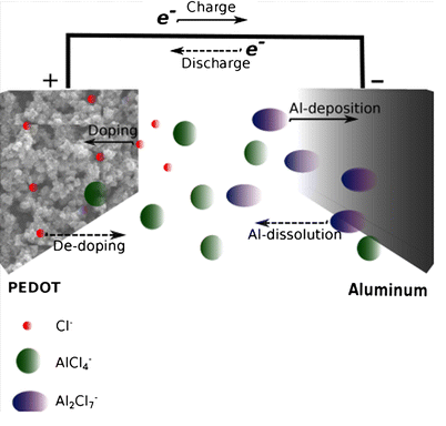
This paper presents a feasibility study of a non-aqueous rechargeable battery based on aluminum and poly-(3,4-ethylenedioxythiophene) conductive polymer in a chloroaluminate ionic liquid. The polymer was electrodeposited on a vitreous carbon working electrode in a chloride aqueous solution and the structure was analyzed by scanning electron microscopy. The doping/de-doping mechanism of chloride ions into the polymer structure was studied using a quartz crystal microbalance and cyclic voltammetry. The deposition/dissolution of the aluminum negative electrode were investigated by electrochemical and microscopic methods.
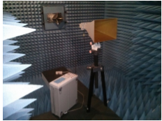
The design of wireless power transfer (WPT) and energy harvesting (EH) solutions poses different challenges towards achieving maximum RF-DC conversion efficiency in these systems. This paper covers several selected challenges when developing WPT and electromagnetic EH solutions, such as the design of multiband and broadband rectifiers, the minimization of the effect that load and input power variations may have on the system performance and finally the most optimum power combining mechanisms that can be used when dealing with multielement rectifiers.

ICON's first year has been very exciting and impactful. We have focussed on setting in motion the recruitment of the Lloyd's Register Foundation Doctoral Students, developing unique programmes that surpass geographical and disciplinary boundaries.
As ICON grows, we will further develop our social media presence for enhancing the public understanding of risk and the new opportunities that nanotechnology brings for making the world a safer place.

The past 70 years have seen the way we live and work transformed by two tiny inventions. The electronic transistor and the microchip are what make all modern electronics possible, and since their development in the 1940s they’ve been getting smaller. Today, one chip can contain as many as 5 billion transistors. If cars had followed the same development pathway, we would now be able to drive them at 300,000mph and they would cost just £3 each.

How resilience engineering could enhance safety through the improved resilience of engineered structures, systems, organisations and communities around the world.
Is nanotechnology the next industrial revolution? Whatever its revolutionary claims the technology is here now. It heralds the ability to manufacture things – materials, components, systems – with atomically precise control. It is the ultimate in miniaturisation; molecular manufacturing.
Get funded, develop & make a difference!

 TWITTER FEED